easyEDA PCB design - avoid this rookie mistake
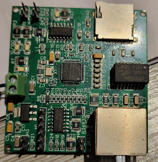
I have been working hard on a project (this one is professional - yes, this blog is highly profitable but I still need to work, but I do it just for fun). I designed and manufactured a few prototype PCBs of the communications portion of my project. I call it "portion" because the main board has a few sub-sections ("portions") and I made separate prototypes of each which I will then join together when I'm happy with each individually.
I don't have loads of experience with PCB design and this project is the first where I have had to make a 4-layer PCB. I struggled to the very end trying to use only the top and bottom layers but finally I had to give up and went for two more. That gave way more breeding room but I had spent so much time optimizing the top and bottom layers that I had relatively few tracks to make on the inner ones.
At the very end of the design I usually make a GND mask on the top and on the bottom and then link the eventual islands using vias. This has served me well in the past but this time it caused me to throw away a bit of money.
As I made the GND vias I looked only at the top and bottom layers. I mean I look at where the GND net is not linked and I will look for a clear path between the top and bottom. When I find that path I usually stick a bunch of vias - not just one - connecting the two and that's it. Well, almost, because now there are the middle layers and I ended up going though a few tracks with my GND vias, effectively connecting a lot of points to GND that should be connected.
Did I not run a DRC (Design rules check)? I did, yes, but not at the very end. Damn, that was stupid! Did the fab house make this anyway? Yes they did with no fault of their own. Ouch.
- Be careful with vias.
- Always run a full DRC at the very end.
- The PCB manufacturer will make whatever you ask - you're in charge.
- Sometimes you make so many mistakes that not even hardware patches can save you.


Comments